
Navitas adds Microchip reference design to its Nvidia 800 V power push
In brief
- Navitas and Microchip unveiled a joint reference design on October 5, 2026.
- Navitas has worked with Nvidia on 800 VDC power semiconductors since May 21, 2025.
- Its 800 V-to-6 V board targets 96.5% to 97.5% peak efficiency.
- Efficiency, density and copper-savings figures are design targets, not proven results.
What the board does
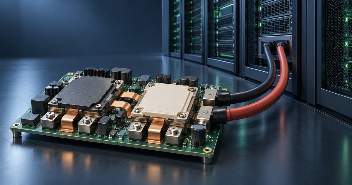
Navitas's work with Nvidia draws on two of its product lines: GaNFast, which uses gallium nitride, and GeneSiC, which uses silicon carbide. The headline product is a direct 800 V-to-6 V DC-DC conversion board. It's designed to skip the intermediate conversion stages that 48 V and 50 V systems have traditionally needed.
The design uses 16 GaNFast FETs rated at 650 V (with 11–17 mΩ specifications). Navitas describes the board as ultra-low-profile, roughly 20% thinner than a smartphone, and it exhibited the hardware at COMPUTEX, which ran from June 2 to June 5, 2026.
The numbers are targets
Navitas says the board is aiming for peak efficiency of 96.5% to 97.5% at 1 MHz switching frequencies, with power densities of up to 2,100 W/in³. The case for the wider 800 V approach is mostly about materials and scale. Navitas points to up to 45% thinner wiring (which works out to a 45% cut in copper needs) along with fewer conversion losses, and the architecture targets 1 MW+ power delivery, compared with traditional systems that top out at hundreds of kW.
None of these are demonstrated results yet.
They're design goals, and real-world deployments will show whether the figures hold at scale. Crypto Briefing's own report makes the same point, so readers shouldn't treat the efficiency claims as settled.
Where Nvidia and Microchip fit
The collaboration plugs into Nvidia's MGX ecosystem and its 800 V HVDC initiative, which covers platforms including Kyber racks and Rubin Ultra GPUs. So what's actually new this month? The Microchip piece.
The joint reference design with Microchip suggests the 800 V ecosystem is drawing in multiple semiconductor players, not only Navitas. That matters for anyone tracking how AI data center power gets built: a single-vendor story is one thing, while a supplier base forming around one voltage standard is a different (and broader) one.
Neither company has given deployment timelines in the material reported so far.
Frequently asked questions
What is the Navitas 800 V-to-6 V board?
It's a direct DC-DC conversion board built for Nvidia's 800 VDC architecture. It's designed to skip the intermediate conversion stages that 48 V and 50 V systems have traditionally needed. The design uses 16 GaNFast FETs rated at 650 V.
Are the board's efficiency figures proven?
No. The 96.5% to 97.5% peak efficiency and the power density of up to 2,100 W/in³ are design targets. Real-world deployments will determine whether they hold at scale.
Why does the Microchip reference design matter?
Navitas and Microchip unveiled a joint reference design on October 5, 2026. It suggests the 800 V ecosystem is drawing in multiple semiconductor players, not only Navitas.