

ASML, TSMC achieve 2D material transistor breakthrough on standard wafers
In brief
- ASML, TSMC, and imec demonstrated scaled complementary transistors using 2D materials on standard 300mm wafers
- 94% yield achieved on next-generation transistors at 50-nanometer contacted poly pitch
- Results presented June 2026 at IEEE/JSAP Symposium on VLSI Technology and Circuits
- 2D materials enable ultra-thin channels without silicon performance penalties at similar dimensions
- Process integrates into existing chip manufacturing flows without back-end modifications
Breakthrough in 2D Materials
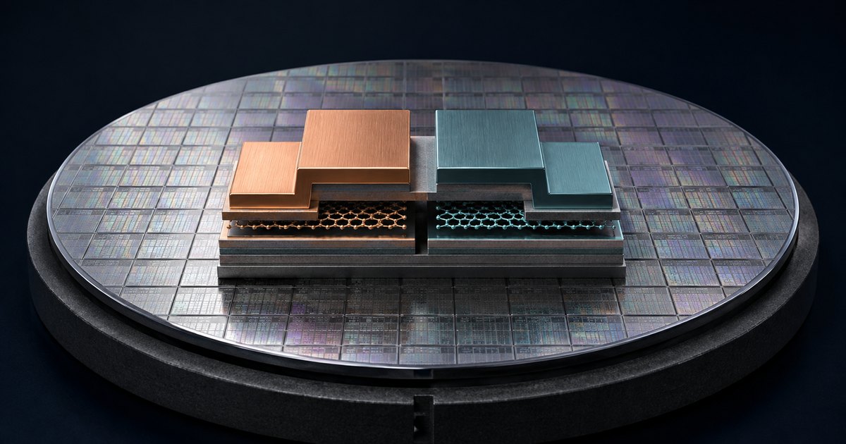
The collaboration achieved a 94% yield on next-generation transistors built from exotic materials. Results were presented in June 2026 at the IEEE/JSAP Symposium on VLSI Technology and Circuits. The team produced both n-type and p-type transistors at a contacted poly pitch of 50 nanometers, using molybdenum disulfide (MoS₂) for n-type channels and tungsten disulfide (WS₂) or tungsten diselenide (WSe₂) for p-type channels.
All transistors were fabricated on industry-standard 300mm wafers using ASML's single-patterning extreme ultraviolet (EUV) lithography. Both transistor types achieved an Imax/Imin ratio exceeding 10⁵ and exhibited very low off-currents at zero gate voltage. The WSe₂-based p-type transistors performed near record levels previously seen only in laboratory settings.
Why 2D Materials Matter
Two-dimensional materials are inherently just a few atoms thick and can form ultra-thin channels without the performance penalties that plague silicon at similar dimensions. This property addresses a fundamental challenge in semiconductor scaling: as traditional silicon transistors shrink, quantum tunneling effects degrade performance. 2D materials sidestep this problem at the atomic level.
The process is back-end-compatible, meaning it could potentially be integrated into existing chip manufacturing flows rather than requiring entirely new fabs. The team noted that their approach is scalable and applicable to other 2D channel materials beyond the three demonstrated.
Remaining Hurdles
Contact resistance between metal interconnects and 2D materials remains a significant integration challenge. Achieving uniformity across an entire 300mm wafer at production volumes will require further breakthroughs. Still, the fact that ASML, TSMC, and imec have moved from laboratory demonstrations to 94% yield on standard wafers signals the transition from proof-of-concept to engineering reality.