Diamond Foundry shows 200mm single-crystal diamond it calls the first at that scale
In brief
- Diamond Foundry showed a 200 mm single-crystal diamond at CarbonSemi 2026 in Ningbo, China.
- Diamond Foundry calls the D200mm the first single-crystal diamond at that scale.
- The D200mm is pitched for cooling AI processors and enabling smaller power electronics.
- The crystal shown was unpolished. Yield and defect density haven't been disclosed.
What Diamond Foundry showed
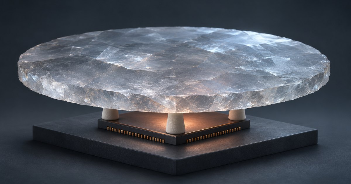
So what's new here? Mostly the size. Diamond Foundry calls the crystal D200mm, and it's twice the diameter of the 100 mm single-crystal wafer the company announced in November 2023. At 200 mm, it also matches the industry-standard wafer dimensions used in chip production. It isn't a polished wafer yet (more on that below).
The structure matters too. The D200mm has one continuous crystal structure, unlike polycrystalline diamond (which is made of many smaller crystals fused together).
Diamond Foundry describes the crystal as the result of 25 years of scientific research and development. It also says its 2022 acquisition of Audiatec, a German firm, sped up progress toward larger crystals.
The AI cooling pitch
Diamond's thermal conductivity is about 2,000 W/mK, roughly five times that of copper, according to Crypto Briefing. That's the core of the company's case. Diamond Foundry is positioning the material for two uses: cooling high-power processors and enabling smaller power electronics. For AI hardware, the company wants the diamond to sit underneath chips and pull heat away from the processors.
Those are the company's stated goals, not demonstrated results.
What hasn't been disclosed
The diamond on display was still unpolished, and Crypto Briefing noted that a raw crystal and a finished, fab-ready wafer aren't the same thing. Diamond Foundry hasn't disclosed yield, defect density or how well the material works with commercial semiconductor processes.
On manufacturing, the company is reported to be developing a $2.77 billion production facility in Spain, a project tied to the EU Chips Act. That's a big commitment. Until Diamond Foundry publishes yield and defect figures, though, the D200mm is a milestone in crystal size, not a production-ready wafer.
Frequently asked questions
What is Diamond Foundry's D200mm?
The D200mm is a single-crystal diamond measuring 200 mm across. Diamond Foundry showed it at the CarbonSemi 2026 conference in Ningbo, China, and says it's the first single-crystal diamond at that scale. It's twice the diameter of the 100 mm wafer the company announced in November 2023.
Why is Diamond Foundry pitching diamond for AI chip cooling?
According to Crypto Briefing, diamond's thermal conductivity is about 2,000 W/mK, roughly five times that of copper. Diamond Foundry wants the material underneath AI chips to pull heat away from processors. It's also pitching the material for smaller power electronics. These are the company's goals, not demonstrated results.
Is the D200mm ready for chip production?
The company hasn't shown that. The crystal on display was unpolished, and Crypto Briefing noted that a raw crystal isn't the same as a finished, fab-ready wafer. Diamond Foundry hasn't disclosed yield, defect density or how well the material works with commercial semiconductor processes.